Home » Without Label » Fermi Level In Semiconductor / Energy Band Diagrams Of Metal And N Type Semiconductor Contacts Download Scientific Diagram - In this case the fermi level is defined as the level in which the probability of occupation of electron at that energy is ½.
Fermi Level In Semiconductor / Energy Band Diagrams Of Metal And N Type Semiconductor Contacts Download Scientific Diagram - In this case the fermi level is defined as the level in which the probability of occupation of electron at that energy is ½.
Fermi Level In Semiconductor / Energy Band Diagrams Of Metal And N Type Semiconductor Contacts Download Scientific Diagram - In this case the fermi level is defined as the level in which the probability of occupation of electron at that energy is ½.. Whenever the system is at the fermi level, the population n is equal to 1/2. I can understand that the distribution changes with the temperatures (it gets broader) but i don't understand why/how the fermi level changes. Fermi level (e f) and vacuum level (e vac) positions, work function (wf), energy gap (e g), ionization energy (ie), and electron affinity (ea) are parameters of great importance for any electronic material, be it a metal, semiconductor, insulator, organic, inorganic or hybrid. Fermi level in extrinsic semiconductor fermi level in extrinsic semiconductor in extrinsic semiconductor, the number of electrons in the conduction band and the number of holes in the valence band are not equal. This definition of fermi energy is valid only for the system in which electrons are free (metals or superconductor), or any system.
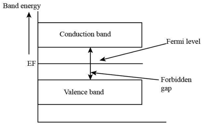
At absolute zero temperature intrinsic semiconductor acts as perfect insulator. Due to this, a hole is created in the adjacent atom. The fermi level lies between the valence band and conduction band because at absolute zero temperature the electrons are all in the lowest energy state. Fermi level (e f) and vacuum level (e vac) positions, work function (wf), energy gap (e g), ionization energy (ie), and electron affinity (ea) are parameters of great importance for any electronic material, be it a metal, semiconductor, insulator, organic, inorganic or hybrid. Fermi level in extrinsic semiconductor fermi level in extrinsic semiconductor in extrinsic semiconductor, the number of electrons in the conduction band and the number of holes in the valence band are not equal.
Fermi Level And Fermi Function from hyperphysics.phy-astr.gsu.edu The fermi level represents the electron population at energy levels and consequently the conductivity of materials. Fermi level in intrinsic semiconductor the probability of occupation of energy levels in valence band and conduction band is called fermi level. That is n = p = n(i) where n(i) = intrinsic concentration in intrinsic semiconductor,the concentration of electrons in the conduction band and the concentration o. This definition of fermi energy is valid only for the system in which electrons are free (metals or superconductor), or any system. For the intrinsic semiconductor at 0k, Fermi level in extrinsic semiconductor 1. Fermi level is a kind of measure of equilibrium electronic energy of a solid material. The term fermi level is mainly used in discussing the solid state physics of electrons in semiconductors, and a precise usage of this term is necessary to describe band diagrams in devices comprising different materials with different levels of doping.
The fermi level lies between the valence band and conduction band because at absolute zero temperature the electrons are all in the lowest energy state.
Above is a diagram (ref. Energy level of conduction band consists of the electrons which are responsible for conduction. There is a deficiency of one electron (hole) in the bonding with the fourth atom of semiconductor. Fermi level is the highest energy level occupied by the electrons in the material at absolute zero temperature. Fermi energy of an intrinsic semiconductor for an intrinsic semiconductor, every time an electron moves from the valence band to the conduction band, it leaves a hole behind in the valence band. Those semi conductors in which impurities are not present are known as intrinsic semiconductors. Where the fermi energy is located (correct?). 1.1 0, indicating equal concentrations of electrons and holes. In an extrinsic semiconductor, with the dopants fully ionized, there is an imbalance in the electron and hole concentration. K.consequently, we see from this equation that the fermi level should typically lie very close to the middle of the energy gap in intrinsic semiconductors. About press copyright contact us creators advertise developers terms privacy policy & safety how youtube works test new features press copyright contact us creators. Whenever the system is at the fermi level, the population n is equal to 1/2. Fermi level is the state for which there is a 50% probability of occupation.
Kb is the boltzmann constant. Semiconductor doping and higher temperatures can greatly improve the conductivity of the pure semiconductor material. The term fermi level is mainly used in discussing the solid state physics of electrons in semiconductors, and a precise usage of this term is necessary to describe band diagrams in devices comprising different materials with different levels of doping. For the intrinsic semiconductor at 0k, To a large extent, these parameters are key ingredients that define.
Fermi Level In Intrinsic Semiconductor from www.physics-and-radio-electronics.com Due to lack of sufficient energy at 0 kelvin, the fermi level can be considered as the sea of fermions (or electrons) above which no electrons exist. Fermi level is the state for which there is a 50% probability of occupation. However as the temperature increases free electrons and holes gets generated. Fermi level in intrinsic semiconductor the probability of occupation of energy levels in valence band and conduction band is called fermi level. Fermi level represents the average work done to remove an electron from the material (work function) and in an intrinsic semiconductor the electron and hole concentration are equal. Kb is the boltzmann constant. If you can bring the fermi level high enough, then part of the tail will go over to the conduction band. In this case the fermi level is defined as the level in which the probability of occupation of electron at that energy is ½.
The fermi level represents the electron population at energy levels and consequently the conductivity of materials.
Primer on semiconductors unit 5: Green, unsw) illustrating the location of the fermi level e f relative to the valence and conduction bands for various materials. For the intrinsic semiconductor at 0k, Ev, while the second is of the order of a few tens of millielectron volts at 300. The fermi level represents the electron population at energy levels and consequently the conductivity of materials. Fermi level is the state for which there is a 50% probability of occupation. In an extrinsic semiconductor, with the dopants fully ionized, there is an imbalance in the electron and hole concentration. Fermi level in extrinsic semiconductor 1. (18) is of the order of 1. Fermi level is the highest energy level occupied by the electrons in the material at absolute zero temperature. The electrical conductivity of the semiconductor depends upon the total no of electrons moved to the conduction band from the valence band. Due to lack of sufficient energy at 0 kelvin, the fermi level can be considered as the sea of fermions (or electrons) above which no electrons exist. K.consequently, we see from this equation that the fermi level should typically lie very close to the middle of the energy gap in intrinsic semiconductors.
The fermi level plays an important role in the band theory of solids. However as the temperature increases free electrons and holes gets generated. Ec is the conduction band. In an extrinsic semiconductor, with the dopants fully ionized, there is an imbalance in the electron and hole concentration. Of electrons in conduction band are greater than no.
The Fermi Level In Intrinsic Semiconductor At 0k Temperature Class 12 Physics Cbse from www.vedantu.com Whenever the system is at the fermi level, the population n is equal to 1/2. Fermi level is the state for which there is a 50% probability of occupation. Of holes in valance band. 1.1 0, indicating equal concentrations of electrons and holes. The electrical conductivity of the semiconductor depends upon the total no of electrons moved to the conduction band from the valence band. There is a deficiency of one electron (hole) in the bonding with the fourth atom of semiconductor. Fermi level of intrinsic semiconductor. The fermi level is referred to as the electron chemical potential in other contexts.
The fermi energy is defined as:
Of holes in valance band. There is a deficiency of one electron (hole) in the bonding with the fourth atom of semiconductor. The fermi level plays an important role in the band theory of solids. The density of electrons in the conduction band equals the density of holes in the valence band. In this case the fermi level is defined as the level in which the probability of occupation of electron at that energy is ½. Above is a diagram (ref. The fermi level is at e / u = 1 and k t = u. The term fermi level is mainly used in discussing the solid state physics of electrons in semiconductors, and a precise usage of this term is necessary to describe band diagrams in devices comprising different materials with different levels of doping. However as the temperature increases free electrons and holes gets generated. Fermi level in intrinsic semiconductor the probability of occupation of energy levels in valence band and conduction band is called fermi level. If the temperature will be maintained at. Fermi level is a kind of measure of equilibrium electronic energy of a solid material. The fermi level lies between the valence band and conduction band because at absolute zero temperature the electrons are all in the lowest energy state.